Terms Used Every Day at Intel
Terminology
Jump to: A-C | D-F | G-J | K-O | P-R | S-U | V-Z
22nm 3-D Tri-Gate transistor
Intel’s 3-D Tri-Gate transistor uses three gates wrapped around the silicon channel in a 3-D structure, enabling an unprecedented combination of performance and energy efficiency. Intel designed the new transistor to provide unique, ultra-low power benefits for use in handheld devices, like smartphones and tablets, while also delivering improved performance normally expected for high-end processors.
A-C
Channel
The region under the gate of a transistor where current flows when the transistor is in the "on" state.
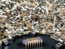
Chip
A tiny, thin square or rectangle that contains integrated electronic circuitry. Die are built in batches on wafers of silicon. A chip is a packaged die. Chips are also called processors and microprocessors. Microprocessors are the brains of computers, servers, communications products, and other digital devices.
Circuit
A network of transistors interconnected by wires in a specific configuration to perform a function.
Cleanroom
The ultra-clean room where chips are fabricated. Cleanroom air is thousands of times cleaner than that in a typical hospital operating room.
Computer-aided design (CAD)
Computerized workstations and software used to design integrated circuits.
D-F
Die
Alternate name for a chip, usually before it is packaged. See also "Chip."
Etching
The removal of selected portions of materials to define patterned layers on chips.
Fab
A shortened term for "fabrication facility," where Intel manufactures silicon chips.
Fabrication
The process of making chips.
Front-opening unified pod (FOUP)
A container that holds and carries wafers as part of an automated system in a fab.
G-J
Gate
The input control region of a transistor where a negative or positive charge is applied to block or allow current to flow.
Gate dielectric
A thin layer underneath the gate that isolates the gate from the channel.
High-k material
A material that can replace silicon dioxide as a gate dielectric. It has good insulating properties and creates a high field effect between the gate and channel. Both are desirable properties for high-performance transistors. Also, because high-k materials can be thicker than silicon dioxide while retaining the same desirable properties, they greatly reduce current leakage.
K-O
Mask
A stencil-like pattern used during fabrication to print layered circuit patterns on a wafer.
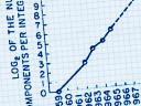
Moore's law
In 1965, Gordon Moore predicted that the number of transistors on a piece of silicon would double every year—an insight later dubbed Moore’s Law. In 1975, Moore updated his prediction that the number of transistors that the industry would be able to place on a computer chip would double every couple of years. As the number of transistors goes up, the cost per transistor goes down.
Nanometer
One billionth of a meter.
P-R
Photolithography
The process of creating a specific pattern of material on a silicon wafer by using UV light and a mask to define the desired pattern.
Photoresist
A substance that becomes soluble when exposed to UV light. Analogous to photographic film, it is sensitive to UV light, but is also resistant to certain etching chemicals. Used to define circuit patterns during chip fabrication.
Polycrystalline silicon
Silicon made up of many crystals, also known as polysilicon. This conductive material is used as an interconnect layer on a chip.
S-U
Semiconductor
A material (such as silicon) that can be altered to conduct electrical current or block its passage.
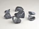
Silicon
The principal ingredient in common beach sand and the element used to make the wafers upon which chips are fabricated. It is a natural semiconductor and is the most common element on Earth after oxygen.
Silicon ingot
A cylinder formed of 99.9999% pure silicon. Ingots are sliced into thin sillicon discs called wafers.
Strained silicon
A layer of silicon that is stretched or compressed to alter the interatomic distance in the lattice. This reduces the atomic forces that restrict the movement of electrons through the transistors. It allows for better mobility, improved chip performance, and lower energy consumption.
Transistor
A type of switch that controls the flow of electricity. A chip can contain millions or billions of transistors.
Ultrabook™
Announced in June 2011 at Computex, the Ultrabook™ device specification, and roadmap changes made to the Intel® Core™ processors are enabling this new breed of devices. Ultrabook systems marry thin and light with the best in performance, responsiveness, security, and battery life—filling the gap between desktop/laptop and tablet.
V-Z
Wafer
A thin silicon disc sliced from a cylindrical crystal ingot. Used as the base material for building integrated circuits.
Wafer sort
An electrical test procedure that identifies the chips on a wafer that are not fully functional.
Zettabyte (ZB)
A unit of computing information equal to one sextillion bytes. (That’s one followed by 21 zeros—enough space to store 4.4. trillion HD movies.) See Gigabytes for other computing units.
Explore Other Online Exhibits
If you can’t make it to the Intel Museum, you can still enjoy a tour of Intel history with these online versions of the exhibits.

Robert Noyce
Intel’s co-founder and the co-inventor of the integrated circuit, he made numerous contributions to the advancement of technology.
Moore's Law
Meet Intel's co-founder and see how his bold prediction set the pace for ongoing innovation.
The Intel® 4004 Chip
Get the story behind Intel’s first microprocessor and learn how it changed the course of technology and the world.
Making Silicon Chips
From purified silicon to technology that powers your everyday life, discover the making of silicon chips—the most complex devices ever manufactured.

Intel Annual Reports and Anniversary Publications
Relive the Intel journey that started in 1968.